By James Schlett
Compared to many of the physical vapor deposition techniques that the optical coatings industry commonly uses, plasma-assisted reactive magnetron sputtering (PARMS) can deliver higher throughput(s) at typically lower costs. In the more than two decades since PARMS tools began to populate the thin-film coatings equipment market, the efficacy of the technique has become obvious to its implementers.
However, compared to these commonly used alternatives — such as ion beam sputtering (IBS), evaporative sputtering, and radio frequency (RF) sputtering — PARMS remains under-celebrated in the optics realm.
Though PARMS does not receive the attention that IBS commands, for example, industry experts suggest that the adoption of technologies for PARMS are more pervasive than widely acknowledged. Further, advancements in integrated photonics, 5G communication, MIR defense applications, and medical diagnostics are leading to opportunities for PARMS to emerge from the shadow of IBS and into the spotlight for critical consumer and defense applications.
Coating process
In 2001, Leybold Optics, headquartered in Alzenau, Germany, developed a sputter tool that incorporated PARMS processes. Three years later, the company commercialized the tool. It was among the first to introduce PARMS capabilities to the optical coatings consumer market, according to Daniel de Sa Pereira, technical sales manager for the semiconductor market at Bühler, which acquired Leybold in 2012.
In PARMS, an additional plasma source that chemically reacts with the atoms from the target material adds to the operation of the regular sputtering process. This type of magnetic sputtering involves the introduction of a reactive gas, such as oxygen or nitrogen, for oxidizing (or nitriding) the coating material. For example, the formation of silica is enabled through the sputtering of silicon and a reactive oxygen plasma step.
PARMS technology has advanced markedly in the last 25 years. “PARMS has, in general, developed into a technology offering some of the most advanced coatings that can be achieved — more than 45 μm [in] deposition up to now — and with very low losses in the film,” said Poul Svensgaard, CEO of Delta Optical Thin Film A/S in Hørsholm, Denmark. “The technology has moved very close to IBS coating, however at a much more attractive price point.”
At the same time, innovations have also served to advance the equipment and machinery associated with the technique, in addition to the underlying technology. Both the industry and research sectors are driving this progress.
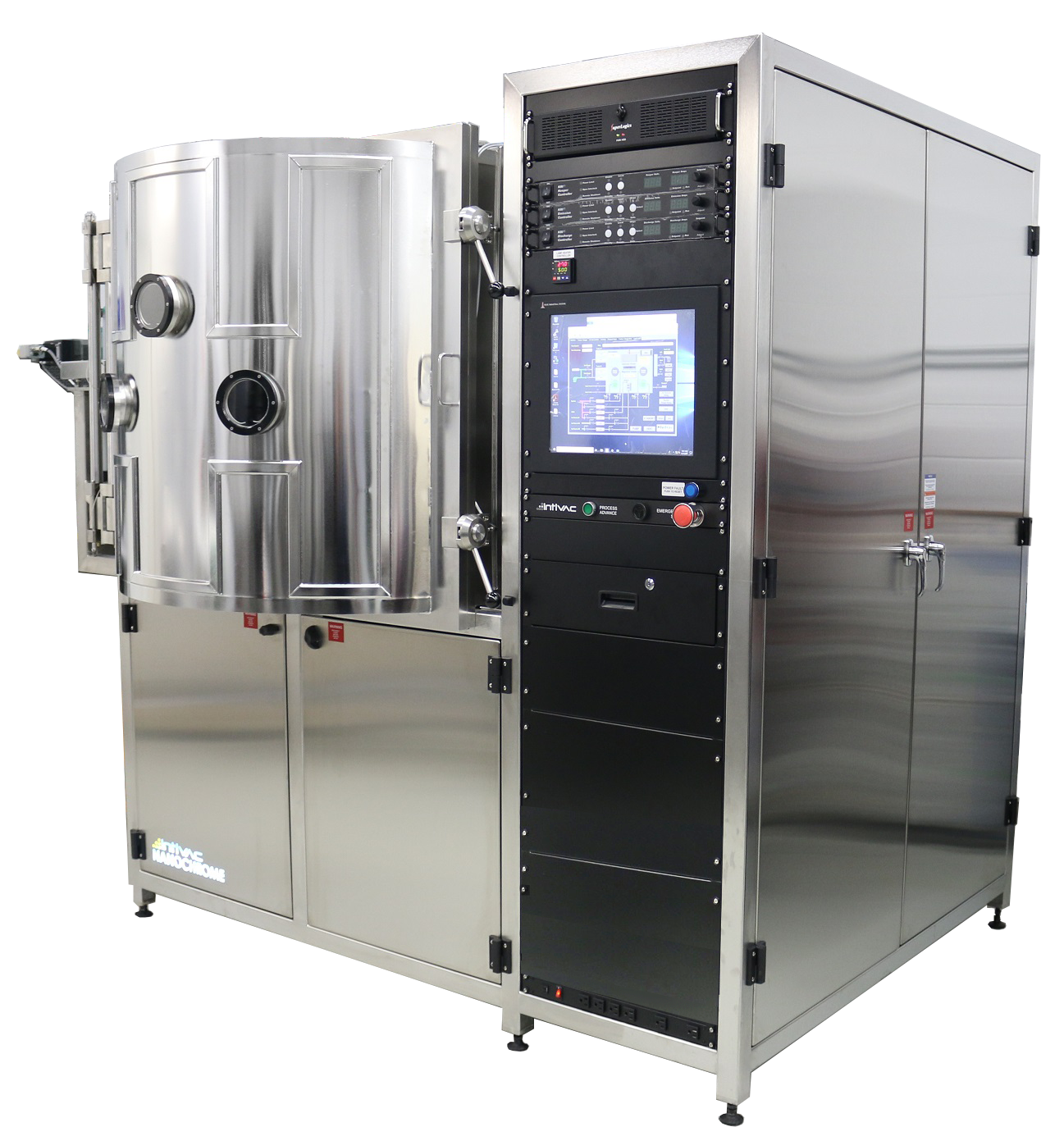
The Nanochrome IV Plasma-Assisted Reactive Magnetron Sputtering (PARMS) system (top) featuring an automatic load-lock mechanism (bottom). Courtesy of Intlvac Thin Film.
Competing techniques
In the early days of PARMS technologies, technical problems such as lack of uniformity and large-particle contamination hindered adoption. In large part, according to Svensgaard, the technology has evolved in such a way that these issues are resolved. PARMS can now offer larger batch sizes, compared to IBS and evaporative/RF sputter techniques, for the same investment in coating machines. It also offers a very stable deposition rate compared to evaporation systems, enabling deposition of thin layers on time and minimizing the need for optical monitoring and re-optimization.
“IBS gets more credit than it’s due, but various [magnetron sputtering] technologies are displacing IBS in many places,” said Peter Egerton, CCO of Alluxa, based in Santa Rosa, Calif. “Several of the key, large champions of IBS coating have moved to off-the-shelf magnetron sputtering technology, which is a bit of a black eye for bespoke IBS technology companies in high-layer-count coatings.”
One key differentiator between PARMS and alternative techniques centers on how each handles the deposition of oxide films. In PARMS, the sputtering is from pure metals, and it reactively forms oxide in the chamber, rather than sputtering from an oxide or relying on evaporation.
Such an approach affords greater control over film purity and composition.
“It is easier to refine gases and liquids to a higher purity than solids, so starting with a pure metal and reacting it with a well-controlled oxygen plasma lets us achieve better results than you’d get from preformed oxide targets,” said Dino Deligiannis, president of Intlvac Thin Film, in Halton Hills, Ontario, Canada. “That is a big part of why PARMS coatings can outperform others in terms of both optical performance and consistency.”
According to Deligiannis, PARMS is “one of the best-kept secrets in the optical coatings industry.”
Yet while many of the companies producing some of the highest-quality optical films in the world are indeed using this technique, they are not advertising their use of it, Deligiannis said.
“The process is more profitable, more flexible, and offers better film quality than a lot of the traditional approaches, especially IBS. So naturally, those already using PARMS would prefer to keep it under wraps,” Deligiannis said.
At Insoptics, a Poznan, Poland-based developer of spectroscopy devices for plasma processes, CEO Artem Artamonov is seeing an increase in demand for coatings in which PARMS can deliver the optimal quality. These areas include dense wavelength-division multiplexing filters for telecommunications, as well as the space and aerospace sector, and for the techniques of fluorescence microscopy, flow cytometry, and DNA sequencing.
At the same time, Artamonov cautioned that companies remain hesitant about undertaking a transition to new technology stacks. Electron beam (e-beam) and IBS methods dominate in the deposition of coatings for these technologies and industries. And efforts to improve quality, stability, and performance are underway for these methods, too.
Performance is only one key measurable. Speed is another. Upstream, additional considerations come into play, according to Artamonov.
“Compared to IBS, PARMS has one significant advantage: the film deposition speed, which is considerably higher,” Artamonov said. “Additionally, it offers simpler scalability of performance due to the ability to create various chamber configurations tailored to different production capacities. For example, there are disk, drum, and standard sputtering PARMS systems. When it comes to e-beam, the main drawback that PARMS addresses is the stability of the refractive index, which simplifies the creation of more complex structures with a greater number of layers.”
Their differences aside, PARMS and IBS both face quality challenges that are primarily related to the accuracy of stopping for each layer — a parameter that depends on both the characteristics of the optical monitor and the operational speed of the equipment. Since PARMS coatings feature hundreds of layers, an error in one can lead to errors in another and degrade the optical performance of the whole coating as a result. Spectral resolution is another area of concern.
And since digital filtering introduces delays in data acquisition, optical signal quality is yet another core consideration.
According to Artamonov, Insoptics addresses digital filtering delays by analyzing all acquired data, including data from previous layers and coatings. “We also suppress cumulative error accumulation by adaptively adjusting layer thicknesses, analyzing the final deposition result at the current error level, and, if necessary, adjusting the thicknesses of the remaining layers,” Artamonov said.
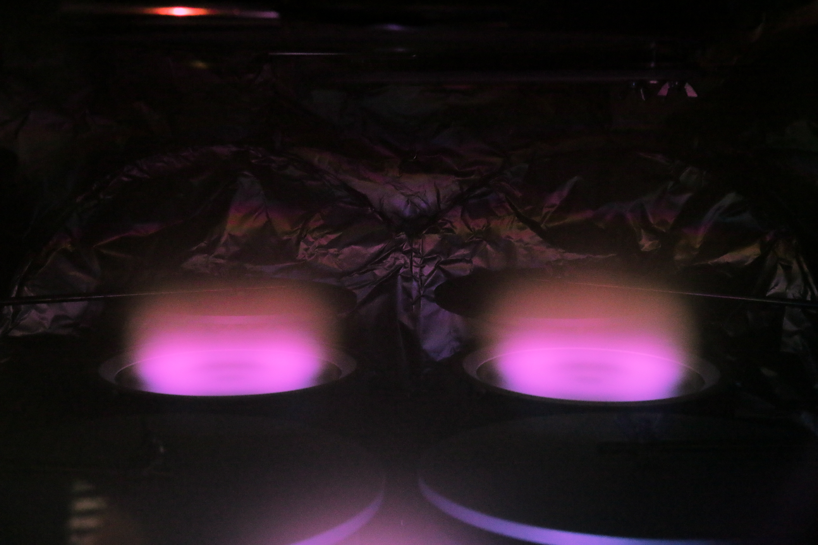
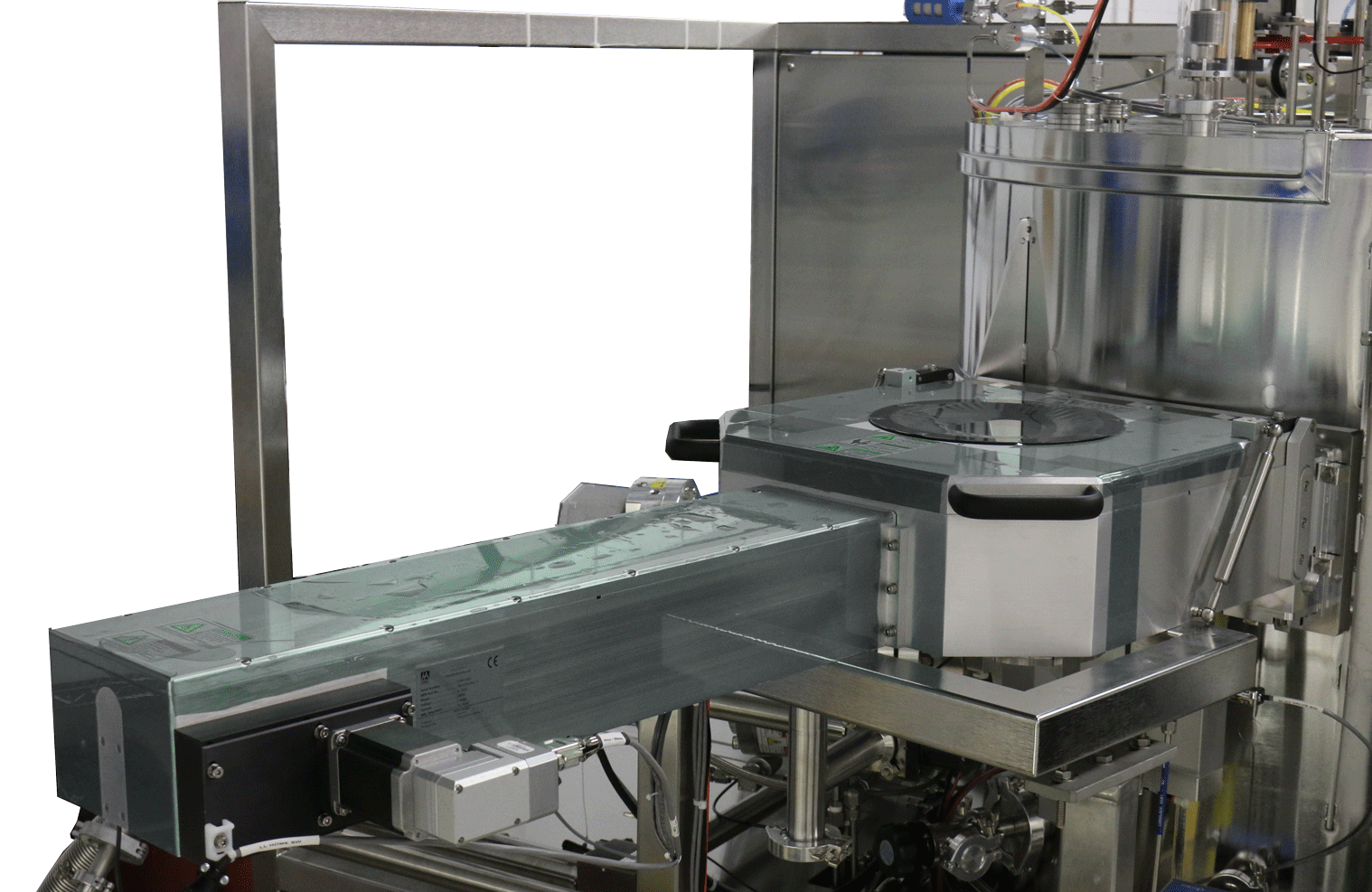
A pure target material reacts with a process gas to deposit a compound thin film (opening image). The reactive sputtering in progress (above). Courtesy of Intlvac Thin Film.
Emerging opportunities
Intlvac’s recent progress in the PARMS-enabled deposition of low-loss aluminum oxide and germanium oxide thin films open the door to applications that use optical waveguides in integrated photonics. For example, using its PARMS process, Intlvac fabricated amorphous waveguides of aluminum oxide at just 150 °C with losses <1 dB/cm at 638 nm and as low as 0.1 dB/cm in the telecommunications band. “This kind of low-temperature, low-loss performance is a big win for applications that require compatibility with temperature-sensitive substrates or CMOS platforms,” Deligiannis said.
Aluminum oxide also has a broad transparency window, spanning the UV to the MIR wavelengths. This is important for many defense applications, at a time when demand from the defense sector has been especially strong for MIR optical filters and laser coatings, Deligiannis said. Svensgaard, meanwhile, said that Delta Optical currently operates in the UV to NIR (300 to 1200 nm) and is expanding upward, toward higher wavelengths.
Jonathan Bradley, an assistant engineering professor at McMaster University in Hamilton, Ontario, Canada, supported Intlvac’s research on aluminum oxide thin films. He said PARMS’ high deposition rates and low-temperature processing allow these materials to be integrated onto sensitive chips, including those fabricated on silicon. In silicon photonics, he said, high temperatures threaten doped layers and metal electricidal contacts. Bradley’s current research is focused on doping materials with light-emitting materials, such as rare-earth metals, which have not been thoroughly explored with PARMS.
Bühler Leybold Optics similarly sees opportunities in optical communications and integrated photonics. The company has focused on the production of dense silica layers that can be used to bond lithium-based wafers to traditional silicon wafers in piezoelectric-on-insulator (POI) structures. With high-quality factor(s), operating frequencies, and device stability, POI currently serves as a base substrate for the next generation of RF-based surface acoustic wave devices used in/for 5G communication.
For the integrated photonics and data communications industries, Bühler is also focusing on the production of silicon nitride via silicon sputtering with reactive oxygen plasma using a nitride gas, according to de Sa Pereira.
“The main advantage that the PARMS offers other than the high uniformity is the tunability of the optical performance — like refractive index — toward the desired target,” he said.
“Moreover, we can produce these films without any hydrogen gas in the process [commonly used in chemical vapor disposition systems], which could be problematic for waveguides used in 1550-nm PICs.”
According to de Sa Pereira, silicon nitride films produced via chemical vapor deposition have a characteristic bond that affects the optical losses of the layer in the infrared. Hydrogen layers are preferred as a result.
Since 2022, when imec qualified its PARMS-based sputter coater machine to meet the environmental standards of semiconductor manufacturing, Bühler has released a third generation of its tool, with a tenfold decrease in particle generation. For silica deposited on a 200-mm wafer, for example, this decrease ensures stable performance of particles sized 160 nm or higher to be <100 adders, or defects caused by particles.
Bühler has also enhanced the full automation capabilities of its sputter coating machinery; the company equipped it with an equipment front-end module capable of opening, loading and unloading, aligning, and detecting wafers from a front-opening unified pod or front-opening universal pod. This feature minimizes operator intervention and significantly reduces the generation of unwanted defects on the coatings, further reducing the cost of ownership, de Sa Pereira said.
Limitations
Limitations remain despite these aforementioned enhancements to PARMS technologies. For example, Svensgaard said that there are no PARMS solutions for ultralow-loss laser mirrors; to his knowledge, IBS is the only available option. And for ultrathin layers that require fully contiguous, subnanometer depositions, atomic layer deposition is the favored technique, Deligiannis said.
Designed as a low-temperature process, PARMS is also not effective when substrate temperatures are required to be between 300 °C and 500 °C, as is the case with high-temperature crystal growth and oriented films. For those applications, traditional RF sputtering with substrate biasing and heating outperforms PARMS, according to Deligiannis.
Film stress, especially when thin glass substrates are involved, is another limitation for PARMS. Though film stress is not a pressing issue for filters that transmit light, it is for mirrors and beamsplitters used in imaging applications that use or require reflection of the image. For such applications, Svensgaard said Delta Optical typically minimizes bending by distributing the coating evenly on both sides of the substrate. According to Deligiannis, Intlvac has largely managed to navigate issues of film stress by controlling ion energy, balancing gas flows, and adjusting temperature. Deligiannis said that the intrinsic stress caused by magnetron sputtering is greater than that from thermal or plasma-enhanced techniques.
Bühler has likewise faced challenges, especially in producing optical coatings on glass wafers with thicknesses of ≤400 μm and 300 mm in diameter. Wafers are at risk of bending or breaking when substrates are coated with layer stacks >1 μm. This demands fine-tuning of the automated PARMS processes to ensure extremely low stress for thin wafers that could feature even slight warpage.
Even in the challenge, there is opportunity. “This could be particularly interesting for metastructure fabrication, where there is a need for optics and their substrates to be miniaturized, or for augmented reality applications, particularly in the fabrication of surface relief gratings used in diffractive waveguides,” de Sa Pereira said.
While there is demand for PARMS coatings with submillimeter thickness and improved spectral performance with fewer coatings, primarily from the defense sector, there are performance trade-offs to consider. “There is a fundamental limit to how thin these coatings can be if you want them to perform,” Deligiannis said. The interference principles that dictate optical coatings production require each layer to be a specific fraction of the wavelength for which it is designed. With IR, that is 250 to 500 nm per layer, with multiple layers needed to achieve individual spectral targets or the desired spectral target range.
Intlvac has focused on making coatings more efficient and durable within those physical constraints. The company has created a higher index contrast by using co-sputtered materials with very different refractive indices to achieve the same spectral performance with fewer pairs. The result is a solution that reduces thickness and ensures that the number of physical layers can be further reduced with more sophisticated designs beyond standard quarter-wave stacks, such as chirped or rugate profiles.
Durability can also be further enhanced by optimizing layer stress, adding barrier layers, and qualifying coatings for long-term exposure to humidity, salt fog, abrasion, and thermal cycling, according to Deligiannis.
“While the request for thinner, fewer, longer-lasting coatings comes up often — especially from military programs — we address it not by trying to cheat the physics, but by pushing materials science and optical design as far as they’ll go,” he said.
Visit Photonics Spectra for more.
Published: September 2025